


A joint white paper by MacDermid Alpha, AMX Automatrix and PreventLab on pressure-assisted silver sintering for SiC power modules: materials, equipment and validation combined into one scalable, repeatable die-attach process.
Pressure Silver Sintering: A Complete Materials, Equipment, and Validation Framework for Modern SiC Power Modules
Authors: Daniele Perico (MacDermid Alpha Electronics Solutions), Alessio Greci (AMX Automatrix), Miriam Vergani and Elena Saglia (PreventLab)
Abstract
Materials, equipment, and validation analyses are essential for enabling power-electronics manufacturers to achieve repeatable pressure-assisted silver-sintering results in thermal and electrical performance and field reliability. This paper presents an integrated framework for silicon-carbide power modules that connects silver-sinter material selection, controlled heat and pressure, bond-line formation, inspection, and qualification. The combined materials–equipment–validation approach is intended to reduce adoption risk, improve process repeatability, and support scalable manufacturing for electric mobility, renewable-energy conversion, industrial power systems, and data-center infrastructure.
Keywords
silver sintering, pressure-assisted sintering, silicon carbide, SiC power modules, die attach, thermal management, reliability, scanning acoustic microscopy
Conflict of Interest Disclosure
This white paper was produced jointly by MacDermid Alpha Electronics Solutions, AMX Automatrix, and PreventLab. All authors are employees of these three commercial suppliers, and the products, equipment, and services described and recommended in this document—including MacDermid Alpha's Argomax silver-sinter materials, AMX Automatrix's pressure-sintering equipment, and PreventLab's inspection and validation services—are commercial offerings of the authors' respective employers. Readers should accordingly weigh the technical claims and recommendations in light of this commercial interest.

High-density power-electronics board illustrating the complexity of modern interconnect demands. Source: MacDermid Alpha Electronics Solutions, 2026.
The market is asking for more current, more heat removal, and more lifetime from the same footprint. The die-attach layer can no longer behave like an invisible commodity step. Power-electronics manufacturers now face a familiar but sharper challenge: while standard consumer electronics are engineered for mild environments with acceptable failure rates, power applications demand uncompromising long-term reliability in harsh environments where failure rates must be strictly maintained well below hard regulation standard criteria.
Power-electronics devices must switch faster, dissipate more heat, and survive longer mission profiles, yet the assembly window cannot become fragile or uneconomic. In that setting, pressure-assisted silver sintering has moved from a promising laboratory concept to manufacturing. The joint question is no longer whether sintering can perform, but whether materials, equipment, and validation can work together tightly enough to make that performance dependable at production scale.
This paper explains why that combined story matters. MacDermid Alpha brings Argomax silver-sinter paste and film platforms designed for die attach, package attach, and related power-electronics flows. AMX Automatrix brings pressure assisted sintering equipment and process control intended to translate material potential into repeatable heat, force, and throughput management.
PreventLab brings capabilities and technical skills to provide a full characterization of sintered junctions for a deep dive into analysis and validation of equipment, materials and processes. Qualification activities identify latent defects not discernible without lab-based examination.
When those three capabilities align, customers gain more than a strong bond line: they gain a clearer path to yield, release confidence, and broader adoption in electric mobility, renewable-energy conversion, industrial power systems, and data-center infrastructure.
Die Attach Thermal Conductivity: The Bottleneck Redefining SiC Power Module Design
Conventional soldering remains important and effective across many package types. Even so, its constraints become more visible as power density, junction temperature, and thermal cycling demands increase.
This becomes increasingly important as silicon carbide (SiC) power devices are adopted in modern power packages designed for electric vehicles, renewable energy systems, industrial drives, and other high-power applications. SiC devices can operate at significantly higher junction temperatures than conventional silicon package devices, increasingly targeting junction temperatures of 200°C, 220°C, or higher depending on the application and reliability requirements.
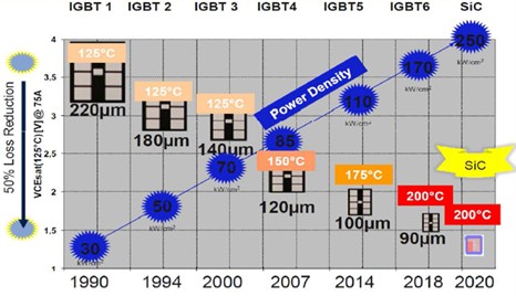
Fig. 01 – Representative concept of increasing power density. Source: D.G. Miller, "Potential of Silicon Power Semiconductor Compared to WBG," ECPE, 2013.
At these elevated temperatures, conventional solder interconnects can become a limiting factor. Many common lead-free solder alloys begin to melt at temperatures near 220°C, while their mechanical strength, thermal-fatigue resistance, and long-term reliability will decline well before the melting point is reached. This can create added risk in applications where repeated high-temperature operation, temperature cycles, and large differences in thermal expansion place stress on the die-attach interface.
Sintered interconnect materials provide a different approach, because sintering forms a solid-state diffusion bond rather than a conventional solder joint. The resulting bond layer is designed for high-temperature stability without the same re-melting concern associated with solder alloys. This can make sintering particularly relevant for SiC packages that must maintain interconnect integrity during sustained high-temperature operation and demanding thermal cycling.
Thermal performance is also key to SiC package design; SiC MOSFETs can switch and manage high power densities, making efficient heat transfer from the die to the substrate essential. A well-controlled sintered bond line can help support a low-resistance thermal path, while consistent bond-line thickness and low voiding are important for maintaining predictable thermal performance across the assembly. The final thermal result will depend on the full package stack, including die metallization, substrate construction, bond-line thickness, void level, and the thermal conductivity of the selected sinter material.
Silicon carbide (SiC) power devices enable higher switching efficiency and power density, but they also raise operating junction temperatures and thermal conductivity. A key advantage of SiC is its wide bandgap, which allows junction temperatures well above 200°C, making the die-attach interface the thermal and mechanical bottleneck. Bulk SiC thermal conductivity varies considerably with polytype and doping level, typically cited across the range of 120–490 W/m·K. For power-device-grade 4H-SiC—the dominant polytype in EV traction inverters and industrial power modules—thermal conductivity at production-relevant doping levels is commonly reported in the range of 120–150 W/m·K, broadly comparable to silicon. The critical thermal design challenge with SiC is not substrate conductivity but rather the combination of higher operating junction temperatures (targeting 200°C and above), higher power density per unit area, and wider thermal cycling ranges encountered in automotive and industrial service conditions. Together, these factors place significantly greater thermomechanical and thermal stress on the die-attach interface and make the thermal resistance, mechanical durability, and fatigue life of that layer a primary design and reliability constraint—which is precisely why the choice of die-attach material and process becomes critical when transitioning from silicon to SiC. As these operating temperatures rise, conventional solder joints operate closer to their melting range and at high homologous temperatures, which accelerates creep and fatigue failure. For example, SAC305 lead-free solder has a melting range of about 217–220°C [12] and is commonly cited with thermal conductivity around ~60 W/m·K. By contrast, pressure-assisted silver sintering forms a solid-state, monometallic joint with thermal conductivity often reported above 300 W/m·K when density is high, and with a re-melting temperature far above typical module operating conditions (bulk Ag melts at 961°C).
The practical implication is a wider reliability and processing window, provided porosity, interface quality, and pressure/temperature uniformity are controlled. Furthermore, the formation of intermetallic compounds—typical of soldering—can increase the brittleness of the joint over time, while repeated temperature excursions can make the connection less resistant to cyclic mechanical stress.
Power module manufacturers push to deliver greater power to the same die area; the joint layer often shifts from being a routine item on the bill of materials to a strategic design constraint.
The Interconnect Paradigm Shift toward pressure sintering is driven by critical performance bottlenecks: excessive interfacial thermal resistance at the die-attach layer, diminishing reliability margins caused by thermomechanical fatigue and the requirement for a stable solid-state connection to support next-generation power package design.
That matters because it changes the engineering approach. Instead of treating die attach as a downstream packaging detail, manufacturers begin to evaluate it as a lever for thermal resistance, switching capability, endurance, and design headroom. MacDermid Alpha states in its power-electronics literature that replacing solder with Argomax sinter material can extend power-cycling endurance by factors of 15–30× in the cited application context, while also supporting higher current with the same die-temperature rise.
This shift also lines up with the broader market. The International Energy Agency describes continued expansion in electric mobility and wider electrification of end markets, while worldwide Departments of Energy continue to frame wide-bandgap power electronics as strategically important for infrastructure, efficiency, and grid performance. Together, those trends raise the value of packaging solutions that can support high thermal conductivity, higher operating temperatures, and stronger lifetime performance without breaking manufacturing economics.
The first value pool is electric mobility. The International Energy Agency reports continued expansion in electric-vehicle markets, and that growth sustains demand for higher-efficiency traction inverters, onboard chargers, and related power modules. In those systems, a lower resistance attach layer, and stronger cycling behavior can directly support thermal margin, package endurance, and switching performance.

Fig. 02 – Transparent EV architecture: silver sintering enables the high-power, high-reliability inverters and power modules that drive electric mobility. Source: MacDermid Alpha Electronics Solutions, 2026.
The second value pool is renewable energy and grid conversion. As electricity systems expand and incorporate more weather-dependent generation, reliable power conversion becomes more important. Inverters, converters, and associated control hardware must handle long service lives, thermal stress, and demanding ambient conditions. A silver-sintering path that improves heat flow and reliability can strengthen the business case for more compact, more robust and more durable conversion hardware.
The third value pool is industrial and data-center infrastructure. MacDermid Alpha emphasizes process flexibility across package sizes and attach formats, while public market analysis from the International Energy Agency points to growing electricity demand linked to electrification and data infrastructure. In this environment, packaging teams need interconnect solutions that help manage heat, preserve operating margin, and fit scalable assembly schemes. Not every data-center power design requires the same package architecture, but many of them reward better thermal paths and more stable long-term interfaces.
The reliability argument for sintered silver is also a sustainability argument. A die-attach layer that supports 15–30× greater power-cycling endurance than conventional solder translates directly to extended product lifetimes, fewer warranty returns, reduced rework energy, and lower total lifecycle carbon impact per power module. As OEMs and Tier 1 suppliers respond to OEM sustainability targets and EU lifecycle regulation, the joining layer is no longer just a thermal and mechanical question—it is an ESG consideration. Argomax silver sintering materials are designed to support higher reliability targets with a reduced environmental footprint relative to repeated solder rework and premature module replacement.

Table 1 and Table 2 – AMX Automatrix Analysis
1. EV Market and Charging Infrastructure Data
- IEA (International Energy Agency) – Global EV Outlook (2024, 2025, and 2026 Editions): primary source utilized for consolidated sales volumes (2023–2024), 2025 data points, and long-term projections.
- EAFO (European Alternative Fuels Observatory): public charging infrastructures and vehicle registration records within EU member states.
- AFDC (Alternative Fuels Data Center – U.S. Department of Energy): historical time-series data mapping the expansion of public and commercial charging stations across USA.
- China Passenger Car Association (CPCA) & CAAM (China Association of Automobile Manufacturers): data source for annual production figures, retail sales, growth rates of New Energy Vehicles (NEVs), and related charging network metrics verified by the China Electric Vehicle Charging Infrastructure Promotion Alliance (EVCIPA).
2. Demographic Data
- Eurostat: official provider of resident population metrics for the European Union.
- U.S. Census Bureau: source for updated demographic data and population records for the United States of America.
- National Bureau of Statistics (NBS) of the People's Republic of China: reference for census and demographic tracking data relative to the Chinese population.
Pressure-Assisted Silver Sintering: The Scalable Answer to Wide Bandgap Power Packaging
In power-device assembly, both solder pastes and sintered-silver systems must manage voiding/porosity because trapped gas or incomplete densification increases thermal resistance and can concentrate stress. For solder pastes, voids form during reflow and can disrupt heat flow in the die-attach layer; published studies and white papers show that void amount and distribution can raise peak temperature and thermal resistance. For sintered silver, some level of porosity is inherent to the process; public DOE-sponsored work shows that key electrical, thermal, and mechanical properties vary with porosity [7], underscoring why pressure distribution, time/temperature, and surface preparation matter. MacDermid Alpha programs often compare candidate interconnects, generating a comparative analysis results database by package type.
Silver sintering changes the discussion because it does not rely on a solder joint: under controlled heat and pressure, silver particles form a dense conductive structure that can support fast heat transfer, strong electrical conduction, and higher-temperature operation.
AMX describes pressure sintering as a die-attach heat-treatment process that increases strength, integrity, and conductivity, and lists benefits such as melting temperature above 400°C, thermal conductivity above 300 W/mK, and strong lifetime-test performance for power-electronics packaging. Major industrial adopters of sintering in volume power modules state that replacing the backside solder layer with silver has dramatically increased the power-cycling lifetime of their modules. Review literature and public reliability work from NREL (2018, USA) [8], Fraunhofer IZM (2020, Germany) and other researchers reach a similar directional conclusion: sintered silver can offer low thermal resistance and excellent cycling behavior when porosity, interface quality, pressure, thickness, and process conditions are well controlled. The important nuance is that sintering is not a single new material introduction; it is a material-process enhanced system. Performance depends on how well chemistry, form factor, tooling, pressure distribution, temperature and inspection logic fit together.
A silver joint is only as scalable as the process window that creates it.
Argomax Silver Sinter Paste, Sintering Equipment, and Process Control: An Integrated Manufacturing System
MacDermid Alpha contributes to the material platform. Its Argomax portfolio includes sinter pastes and films for die attach, top attach, package attach, and wafer-related flows in power electronics. The company highlights low-pressure sintering enabled by proprietary nano-particle technology, film formats for die and clip lamination, and process flexibility across dispense, print, laminate, and wafer-level approaches. In its 2025 power-electronics internal literature, MacDermid Alpha also describes film-based flows that allow heated dies to be laminated, then placed and sintered directly onto direct bonded copper substrates or copper leadframes. That matters because it reduces variability associated with some print-and-dry sequences while enabling a cleaner and more repeatable bond-line strategy in selected applications.
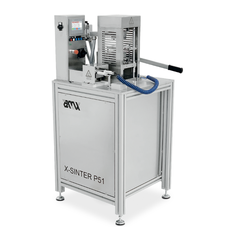
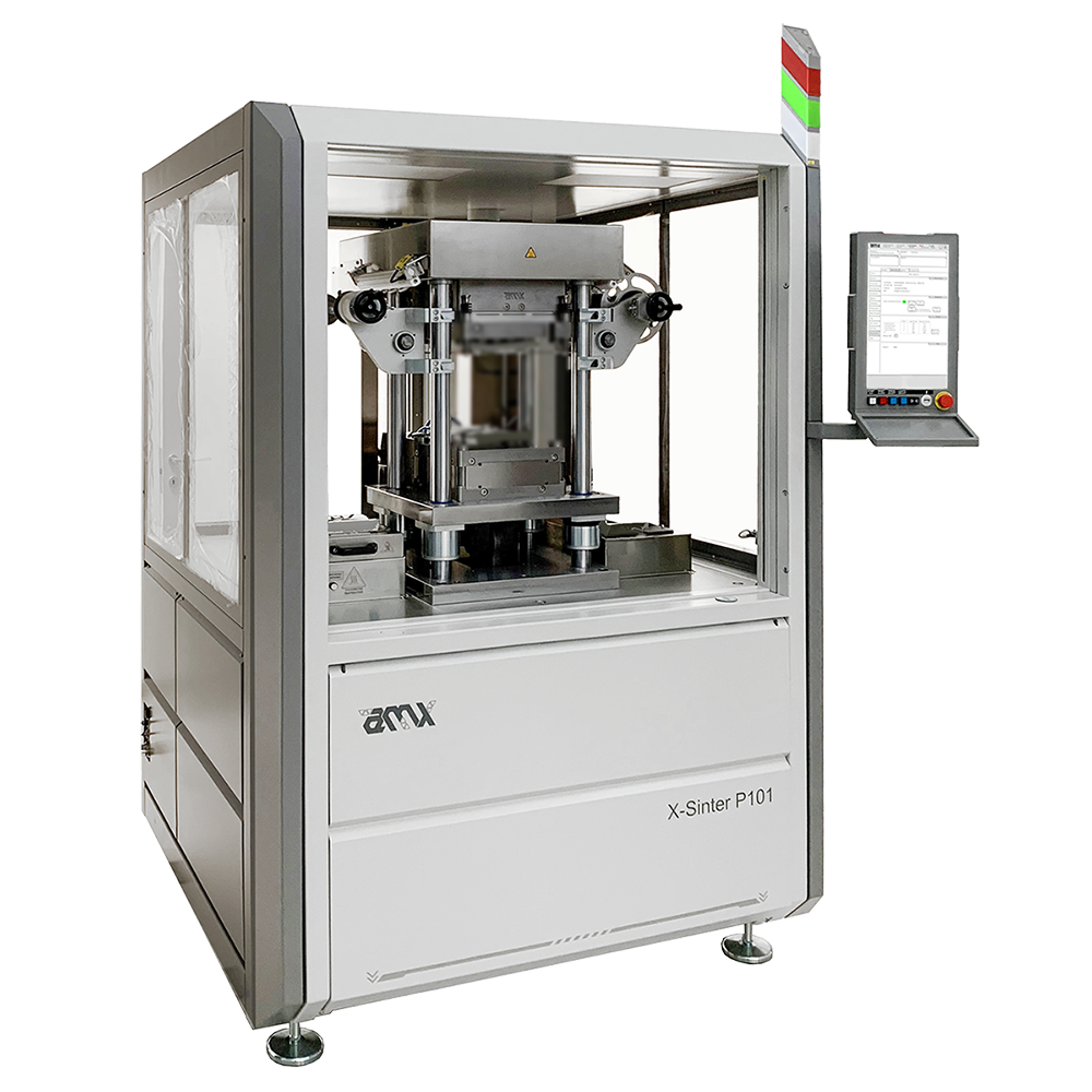
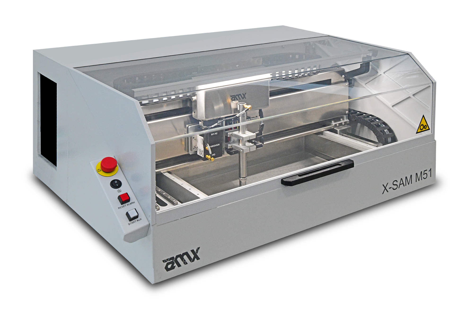
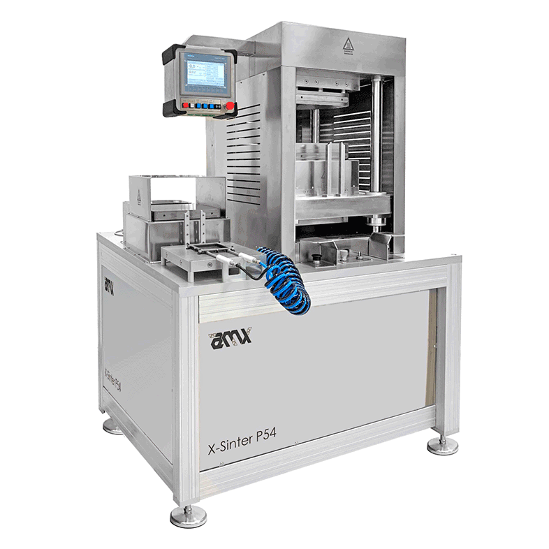
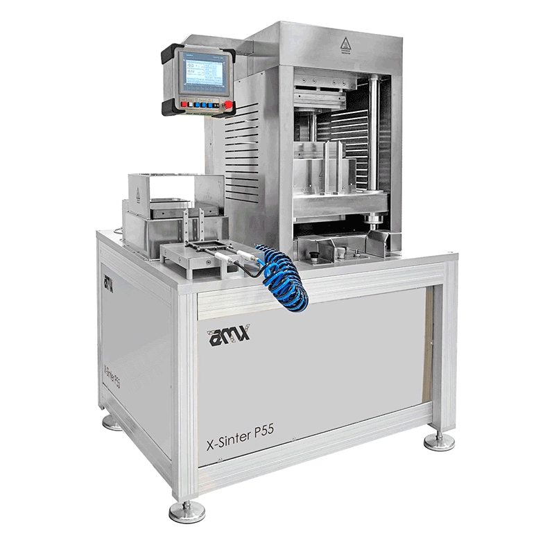
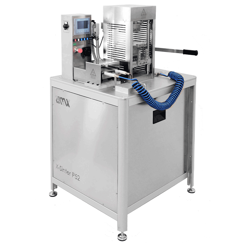
AMX contributes to the process discipline. Its X-Sinter platform family addresses die sintering on ceramic substrates, clip sintering, leadframe applications, double-side-cooled packages, large-area sintering, and wafer-level flows. AMX is also known for its patented Micro-Punch system that can press each individual component with dedicated pressure. That capability is especially relevant in real modules, where component mix, local height variation, and geometric complexity can challenge uniform densification. Dedicated local force control can help translate a good material into a more consistent structure across the full substrate rather than a best-case coupon result.
The PreventLab approach consists of taking a preventive strategy at the design stage to enable custom-fit solutions and reliability outcomes that optimize time, cost, energy consumption, and minimize field returns. Beyond standard validation, PreventLab is fully equipped to provide comprehensive failure analysis and diagnostics to identify problems' root cause and implement appropriate corrective actions.
This explains why the strongest joint message for customers is not "paste" or "press" alone. It is the pairing of the right silver system with the right process architecture. This is where a joint paper becomes stronger than a single-supplier story.
For customers, the practical benefit is clear. A joint materials-and-equipment message reduces adoption risk. Instead of hearing two separate claims, the customer hears one connected manufacturing logic: the chemistry is tuned for the attach problem, the tooling is tuned for pressure control, and the combined process is designed to reach a stable outcome on real hardware. That is a stronger commercialization story than performance language alone.
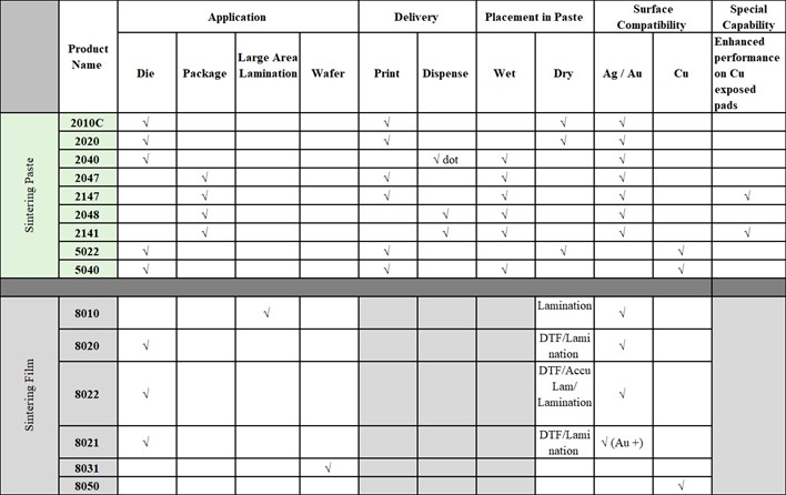
Table 03 – Author's contributions. Source: MacDermid Alpha Electronics Solutions, 2026.
Argomax History and Material Platform: Pastes, Films, and Preforms
Argomax is MacDermid Alpha's silver-sinter technology platform for power-electronics interconnects, offered in multiple formats to match different applications and assembly flows. The portfolio includes paste and film products for die attach, top attach and package attach, and has expanded over time as power-module architectures and throughput needs evolved. Constant product portfolio updates (e.g., Argomax 2148 for EV power inverters) illustrate ongoing extension of the platform for larger packages and demanding surfaces. Across the range, the goal is to deliver a pure-silver bond line with high thermal/electrical performance using manufacturable, often low-pressure sintering processes.
Not all silver sintering pastes offer low-pressure processing capability. Argomax nano-particle technology enables sintering at applied pressures significantly lower than those required for conventional micron-particle formulations. This reduces mechanical stress on sensitive die metallization, extends the range of compatible package geometries, and lowers capital requirements for the sintering press. For manufacturers evaluating sintering as a solder replacement, the sintering pressure requirement is often the first process integration constraint—and it is where material particle design has a direct impact on process window and tool specification.
Argomax pastes support dispensing or stencil printing and can be tuned for rheology, wet die placement, and drying behavior. Argomax films (e.g. Argomax 8022, latest Acculam solution) can reduce bond-line thickness variation, simplify handling for large die areas, and enable lamination-based workflows that improve repeatability in high-volume assembly.
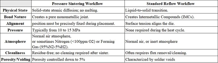
Table 04 – Author's contributions. Source: MacDermid Alpha Electronics Solutions: product portfolio of silver sintering pressure-assisted materials.
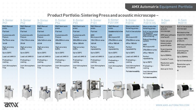
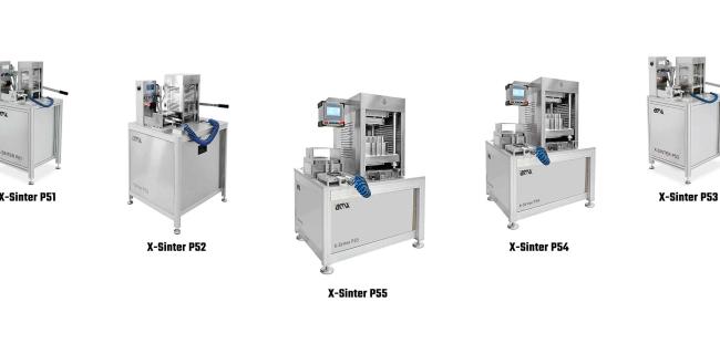
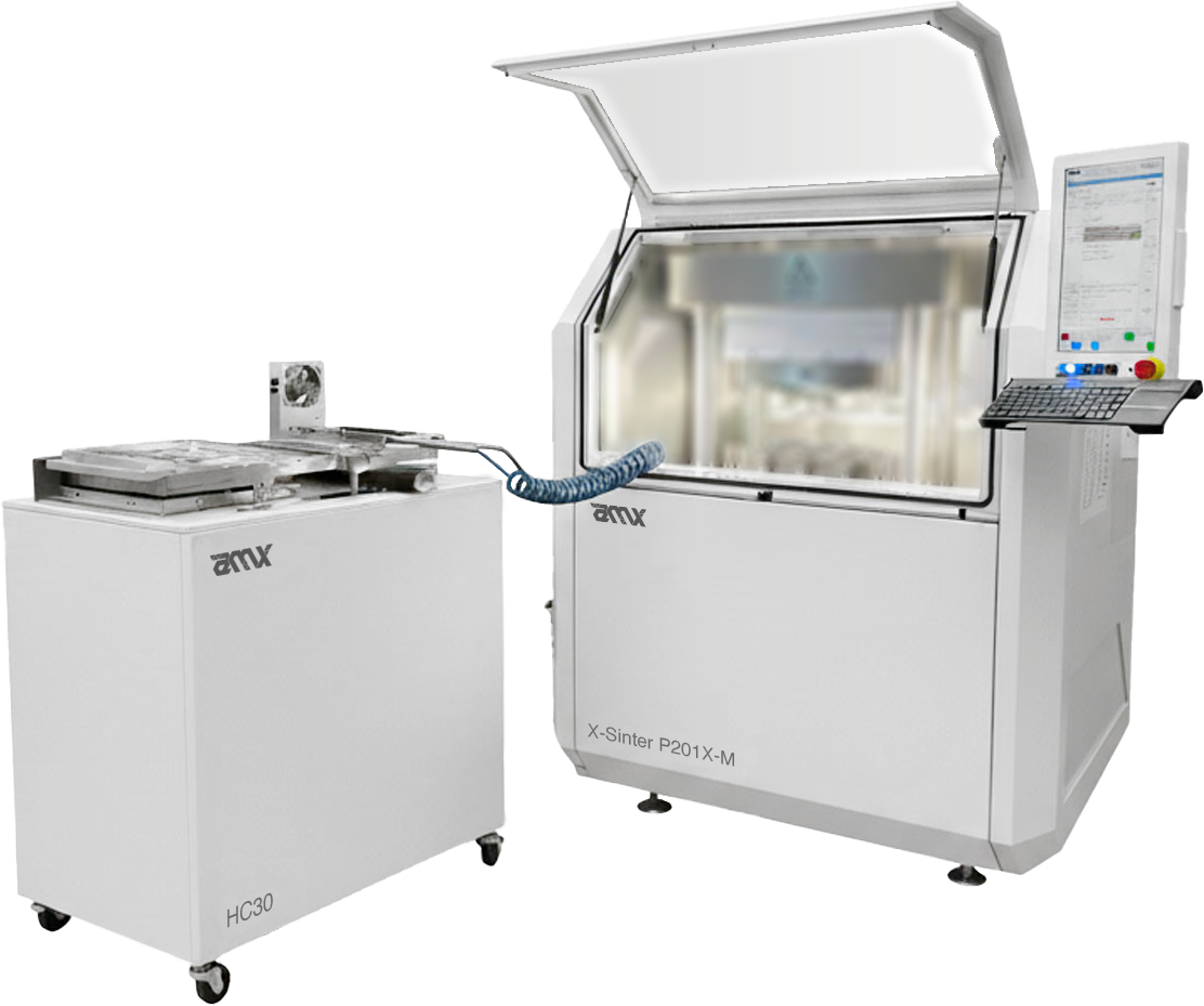
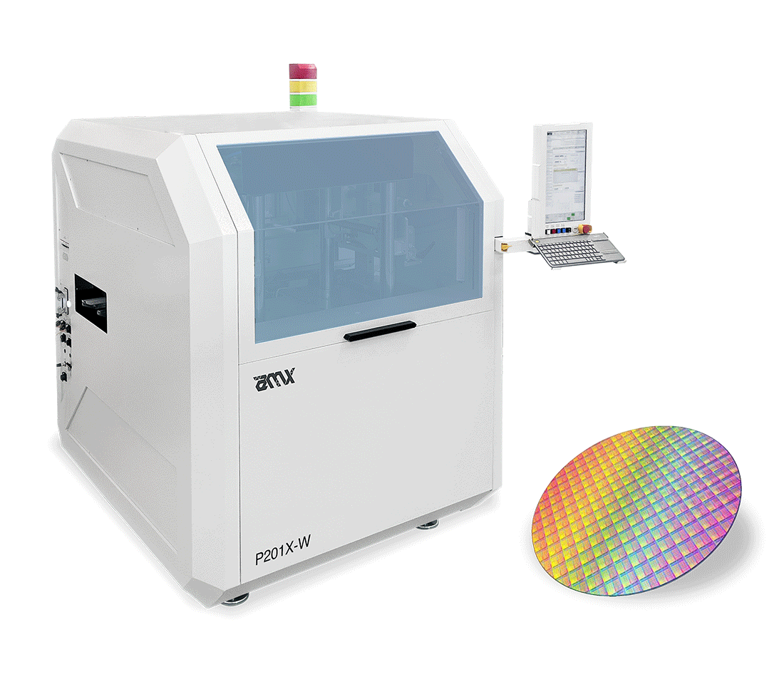
Fig. 03 – AMX Automatrix equipment portfolio, July 2026. Source: AMX Automatrix, 2026.
Pressure-Sinter Process Workflow
Soldering is a liquid-to-solid transition process designed for high-volume, self-aligning assembly that includes Solder Deposition (solder paste is printed onto the board), Component Placement onto the wet paste using standard pick-and-place equipment, and a Reflow Profile through a multi-zone tunnel oven where temperatures exceed the alloy's melting point (typically ~220°C for SAC solders). During the molten phase, surface tension causes the component to pull into alignment with the pads. At the same time the solder forms intermetallic compounds (IMCs) with the components.
Sintering is a solid-state diffusion process used to form dense, reliable interconnects. For sinter paste assembly, the most common approach is Dry Placement, in which the paste is dried before the component is placed. This step removes solvents before pressure sintering and will help to reduce paste squeeze-out, component movement, and void formation.
A typical Dry Placement workflow for sinter paste assembly includes the following steps:
- Stencil Printing: silver (Ag) or copper (Cu) sinter paste is printed onto the substrate, typically a DBC or AMB substrate, using a customized stencil designed for the required deposit geometry and bond-line thickness.
- Pre-Drying: the printed paste is dried before die or component placement, in an oven at approximately 100–150°C. Depending on the surface finish, a nitrogen atmosphere can be beneficial. This removes solvents and helps prepare the paste deposit for controlled placement and pressure sintering.
- Die Placement: components are positioned onto the dried paste deposits. Depending on the assembly and equipment configuration, hot tacking can be used to promote initial adhesion and help maintain die position during transfer and handling.
-
Sintering Cycle: the assembly is processed in a dedicated sinter press. It consists of:
- Preheating: the carrier and assembly are heated to a temperature well below the sintering temperature, commonly in the range of 80°C–120°C.
- Pressure Application: controlled pressure and heat (typically in the range of 240°C–275°C) is applied to promote particle densification and bond formation. Equipment with individually controlled actuators can help compensate for die-height variation and support consistent pressure distribution across multiple devices. The pressure depends on the die or package type, but normally varies from 8 to 20 MPa.
- Post Cooling: the assembly is cooled under an inert atmosphere, particularly where oxidation control is important for copper-containing components or metallization.
- Downstream Assembly and Characterization: after sintering, the assembly may proceed to wire bonding, encapsulation, and other package-assembly steps. Non-destructive characterization methods, including Scanning Acoustic Microscopy (SAM), may be used to assess delamination, voiding, and interfacial integrity.
As an alternative to the above process, the Wet Placement process may also be used in certain applications. In this approach, components are placed directly onto the undried paste, and drying occurs after placement, offering also a beneficial self-leveling effect. In addition to this, wet placement can offer advantages in certain specific conditions: substrate geometries, die sizes, or production flows, but it requires careful process control to prevent paste displacement and trapped volatiles during the subsequent drying and sintering stages.
For some applications, Argomax Die Transfer Film can provide an alternative to stencil printing and pre-drying. The film format can simplify material handling, provide process tack for die placement, and support more predictable bond-line thickness control.
All these applications result in a similar bond: a strong reliable silver layer with a controlled level of porosity, which is essential for buffering against CTE mismatch between the components in the stack.
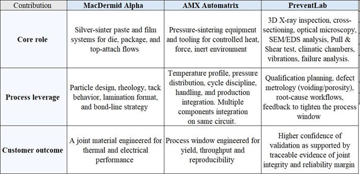
Table 05 – Author's contributions. Comparative process description: pressure sintering vs pressureless.
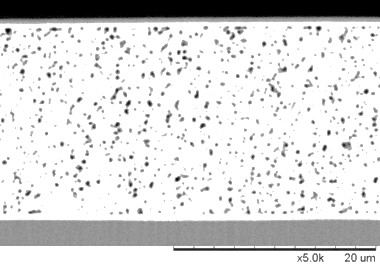
Fig. 04 – Cross-section of Ag layer, pressure-assisted, highlighting porosity of the material: 15 MPa pressure sintering, porosity <5%. Source: MacDermid Alpha Electronics Solutions, 2026.
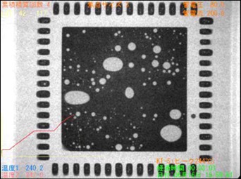
Fig. 05 – Voids propagation during reflow soldering. Source: MacDermid Alpha Electronics Solutions, 2026.
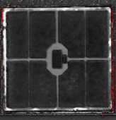
Fig. 06 – SAM inspection 100 MHz IGBT after pressure sintering, almost 0% voids rate. Source: AMX Automatrix, 2026.
AMX Equipment Technology
The AMX MicroPunch system can sinter all the architectures including: HPD and T-pak die on substrate, clips on top of the die, embedded and 3D architectures, due to its individual control and zero punch gap.
- Compensation: the AMX® MicroPunch system can compensate for height variations and substrate non-planarity up to ~±250 µm, ensuring that every component—even at different depths—receives the exact target pressure;
- Different Force Ratios: unlike flat tools, MicroPunch allows for different pressure ratios within the same cycle. For instance, it can apply 15 MPa on the SiC dies while simultaneously applying only 8 MPa on sensitive NTC sensors or IGBR resistors to prevent structural damage;
- Tilting Control: it maintains die tilting to less than ±5 µm, ensuring a homogeneous Bond Line Thickness (BLT), which is critical for thermal conductivity in high-density modules.
In addition to this, in order to support the Automotive standard AQG 324 (ECPE) as a reference, it is important to guarantee reliability and repeatability of the process and in particular to have good temperature control to avoid deviation, and pressure distribution to avoid poor sintering of components placed on the peripheral area of the tool.
Atmosphere Control and Copper (Cu) Sintering
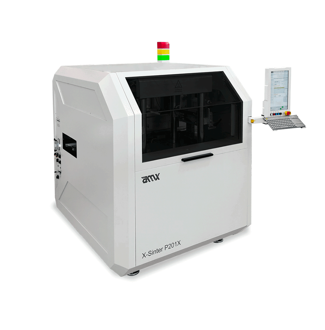
For high-integrity monometallic joints, the X-Sinter P201X full inert atmosphere cabinet provides a certified controlled oxygen-level environment, with a certified sensor capable of operating up to 100 ppm O2.
The system utilizes an insulated cabinet with nitrogen (N2) protection covering the entire workflow: preheating (from room temperature to typically ~120°C), tool operation (up to 320°C), and post-cooling (back again to room temperature, avoiding after-process cosmetic defects).
AMX can also manage the reducing atmosphere (Forming Gas), which becomes thermochemically active above 250°C to reduce surface oxides (CuO). Thanks to this unique concept, the equipment is capable of avoiding any cosmetic defect on exposed copper areas and copper components, and at the same time it guarantees the possibility to work in the future also with copper thermal interface materials.
Die Attach Validation: Power Cycling Endurance Testing and Structural Qualification
Structural inspection closes the second half of the loop. PreventLab describes a series of analytical activities that enable the identification of macro-defects and latent micro-defects, thereby ensuring complete product and process validation. Inspection and analysis help explain why it works, where the margin sits, and where the process still needs tightening. PreventLab offers different kinds of recommended tests and analysis for power electronics for complete characterization. Qualification typically combines non-destructive inspection, destructive verification, and accelerated stress testing. Failure analysis should close the loop by mapping defects and crack paths back to process settings so the manufacturing window can be tightened.
Recommended analyses include:
- 3D X-ray (CT)
- Cross-sectioning / Optical microscopy (OM)
- Scanning Electron Microscope (SEM) and Energy Dispersive X-ray Spectroscopy (EDS)
- Die Shear test
- Aging chambers (static, thermal shock/cycling, vibrations)
3D X-ray could be suited for a non-destructive and raw characterization of sintering joints as it discerns macro-defects (such as relevant voids, cracks, lack of material) but it cannot provide details, despite its high resolution (0.1 µm/pixel), about micro-defects (such as fine voids/porosities and small cracks/separations). This technique is often associated with Scanning Acoustic Microscope (SAM) analysis, which however shares the same limitation about micro-details.
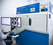
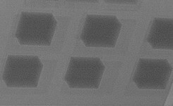
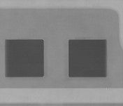
Fig. 07–09 – PreventLab X-ray analysis of sintered joints. Source: PreventLab, 2026.
The most powerful technique, capable of achieving the highest spatial resolution and assessing critical insights into internal quality, is cross-sectioning.
The process typically involves sectioning the sample, embedding it in a rigid resin (mounting), and progressively grinding and polishing the surface to a mirror-like finish.
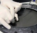
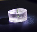

Fig. 10–12 – PreventLab micro-section analysis. Source: PreventLab, 2026.
This eliminates surface artifacts and prepares the sample for high-resolution imaging, usually via Optical Microscopy (OM).
It allows for a detailed evaluation of the joint's microstructure, revealing porosity distribution, bond line thickness (BLT) measurement, and potential delamination at the interfaces.
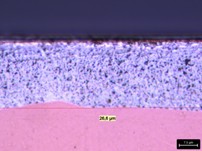
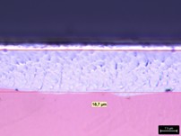
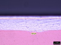
Fig. 13–15 – Micro-section images of Argomax film after sintering by different process parameters (combination of temperature, time and pressure) and BLT measurements by OM imaging. Source: PreventLab, 2026.
The cross-section sample could be further investigated by Scanning Electron Microscopy (SEM) and Energy Dispersive X-Ray Spectroscopy (EDS), which provide morphological analysis at high magnification of sintering/bonding interfaces and their elemental compositional analysis too.
SEM Analysis: Microstructural and Morphological Evaluation
Because sintered silver is a porous matrix, high-magnification SEM imaging is essential to evaluate the sub-micron physical features of the joint.
In a typical failure analysis or process optimization workflow, SEM focuses on:
- Porosity and Densification Mapping: SEM allows for the quantification of the ratio between silver grains and empty voids (pore size distribution). A high initial density correlates with superior mechanical shear strength and thermal conductivity.
- Grain Growth and Coalescence: during high-temperature aging, the silver sub-micron particles tend to minimize their surface energy by merging into larger grains. SEM cross-sectional imaging tracks this morphological evolution, which can lead to localized stress concentration.
- Micro-crack and Void Propagation: SEM is used to inspect cross-sections of joints that failed during die shear testing or thermal fatigue. It identifies whether cracks propagated through the bulk of porous silver (cohesive failure) or along the boundary layers (adhesive failure).
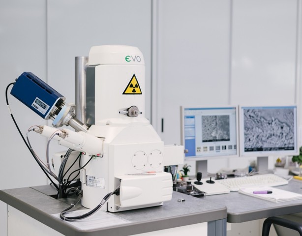
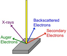
Fig. 16–17 – SEM/EDS technique allows surface reconstruction by SE (secondary) or BSE (backscattered) electrons and compositional analysis by X-ray emission. Source: PreventLab, 2026.
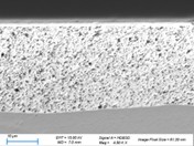
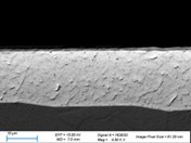
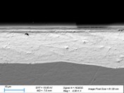
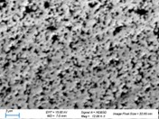
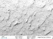
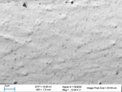
Fig. 18–23 – Micro-section images of Argomax film after sintering by different process parameters by SEM BSE imaging. Source: PreventLab, 2026.
EDS Analysis: Chemical and Interfacial Characterization
While SEM provides topography and morphology, EDS provides spatial elemental composition by detecting characteristic X-rays emitted from the sample when bombarded by SEM electron beams.
For silver sintering, EDS is critical for:
- Interfacial Diffusion and Intermetallic Compound (IMC) Identification: silver is often sintered onto substrates or dies metallized with Gold (Au), Copper (Cu), or Palladium (Pd). EDS line scans or element maps reveal the diffusion depth of Ag into these layers and detect the formation of specific phases or unwanted oxidation at the boundaries.
- Electrochemical Migration (ECM) Diagnostics: when samples fail temperature-humidity-bias (THB) tests in climatic chambers due to short circuits, EDS is used to scan the dendritic structures growing across isolation gaps. This confirms whether the conductive dendrites are composed of purely migrated silver or silver oxides/sulfides.
- Contamination Detection: trace amounts of organic residues from the original sintering paste (binders/dispersants) or atmospheric contaminants (such as Sulfur or Chlorine) can be localized and identified via EDS point analysis, helping to isolate the root cause of premature joint embrittlement.
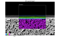
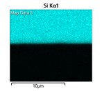
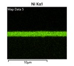
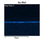
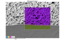
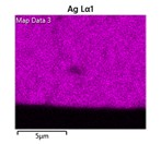
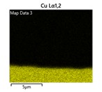
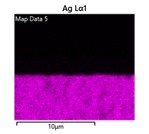
Fig. 24–31 – EDS mapping of Argomax film after sintering, which shows the disposition of elements revealed by X-ray emission supplied by the EDS spectrometer. Source: PreventLab, 2026.
Die shear testing is a destructive mechanical evaluation method used to quantify the adhesion strength and structural integrity of silver-sintered interfaces. In power electronics, this test is critical both for optimizing the initial sintering process parameters (such as pressure, temperature, and time) and for assessing the mechanical degradation of the joint after environmental aging in climatic chambers. Die shear test could characterize:
- Cohesive Failure: the fracture occurs entirely within the bulk of the porous silver sintered matrix. This indicates excellent adhesion to the bounding layers and means the measured strength reflects the intrinsic mechanical properties of the sintered silver.
- Adhesive Failure (Interfacial): the separation occurs at the interface between the silver layer and the die metallization (e.g., Ag, Au) or the substrate. This often points to poor surface preparation, insufficient sintering pressure, or severe intermetallic degradation during thermal aging.
- Mixed Mode Failure: a combination of cohesive and adhesive failure, which is the most common outcome after long-term cyclic stress in climatic chambers.
In the context of silver sintering, climatic chambers shift the focus from mere material characterization to prognostics and health management (PHM), intended as a discipline focused on assessing the real-time degradation of a system, predicting its remaining useful life (RUL), and preventing catastrophic failures.
They provide the empirical data necessary to validate lifetime prediction models, ensuring that high-power electronic modules can withstand decades of environmental and operational stress without interface failure.
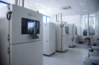
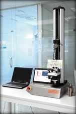
Fig. 32–33 – Aging chambers and Pull & Shear equipment. Source: PreventLab, 2026.
In-Line Control: AMX Scanning Acoustic Microscopy (X-SAM) and SPEA Automatic Test Equipment
To certify zero-defect manufacturing of power module packages, AMX has for years believed that the preferred method is the use of ultrasonic inspections. Operating at frequencies typically from 5 MHz up to 400 MHz (1 GHz for other applications), the X-SAM detects delamination and voids. The inspection mainly consists of analyzing the phase difference of ultrasonic waves between the different materials that compose the package (such as ceramic/SiC/silver/copper layers) and the air or empty spaces of micro-defects given by delamination or cracks. It detects defects up to a 10 µm pixel resolution, providing 100% inspection capability in mass production (M201X model) to ensure the integrity of the monometallic interconnection.
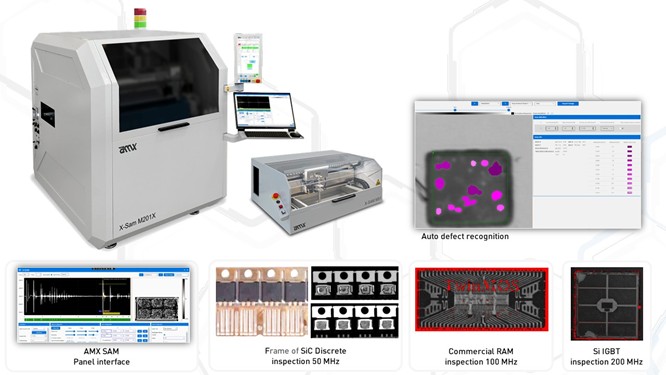
Fig. 34 – SAM equipment and analysis results. Source: AMX Automatrix, 2026.
High-performance packaging programs do not earn release confidence through attach strength alone. They earn confidence through measurement, inspection, and failure understanding. This is why the broader validation layer matters. SPEA highlights that ensuring the reliability of power electronics—especially with the rise of Wide Bandgap materials like SiC and GaN—requires a comprehensive, full-chain testing strategy. While advanced packaging processes like sintering establish structural integrity, SPEA's testing solutions validate performance from wafer and singulated dies (KGD) up to fully assembled power modules and boards. This multi-core, high-power test infrastructure intercepts latent parametric drifts, successfully guiding manufacturers toward a true zero-defect production reality.
Credibility grows when the joint is not only built, but measured, inspected, and understood.
This matters commercially and technically. Journalists, analysts, and buyers respond better to a manufacturing story that includes validation logic. A credible joint paper therefore should not stop at materials and sintering equipment. It should show that the resulting structure can be electrically verified, physically inspected, and refined with data. That is how a promising process becomes a release-ready solution.
Silver Sintering That Scales: The Materials-Equipment-Validation Advantage for Power Electronics Manufacturers
The strongest joint position for AMX and MacDermid Alpha is not simply that silver sintering performs well. The stronger claim is that high-performance sintering can be made more manufacturable when material design and process control are developed as a connected stack. MacDermid Alpha supplies silver systems built for practical assembly routes, including paste and film options that address different production needs. AMX supplies the thermal and mechanical discipline needed to turn those materials into repeatable joints across real device geometries. Add test and analysis, and the customer sees a full path from attachment to proof.
That message creates value on four levels. First, it frames the market problem in business terms: hotter modules, tighter reliability windows, and rising pressure on package efficiency. Second, it states the value proposition in engineering terms: lower thermal resistance, stronger cycling potential, and a wider process window when the stack is aligned. Third, it confirms value with evidence from official product literature, industrial adoption, and public reliability studies. Fourth, it gives the reader a practical next step: evaluate the joint process on a representative customer design, with shared material, equipment, and validation support rather than a fragmented handoff.
Customers do not buy a bond line. They buy cooler operation, longer lifetime, cleaner qualification, and a faster route to production confidence. For engineers and procurement specialists evaluating pressure-assisted silver sintering for SiC die attach, die package attach, or wide-bandgap power module applications, MacDermid Alpha, AMX Automatrix, and PreventLab offer a joint process evaluation pathway: from material selection and process optimization through inspection and qualification. To request a consultation, sample materials, or a process trial on your representative package design, do not hesitate to contact the contributors.
About the Contributors
MacDermid Alpha Electronics Solutions
MacDermid Alpha Electronics Solutions (MAES) develops electronics assembly and semiconductor packaging materials, including ALPHA® Argomax® silver-sinter pastes and films for power-electronics interconnects. The Argomax portfolio supports die attach, top attach, and package attach flows, with options designed for manufacturable low-pressure sintering and repeatable bond-line control.
Contact: https://www.macdermidalpha.com/contact-us
Website: https://www.macdermidalpha.com
Corporate HQ: 245 Freight Street, Waterbury, CT 06702, USA
AMX Automatrix
AMX Automatrix, established in 2011 by Copromec Group, specializes in tailored automation solutions for the electric-automotive industry, with headquarters in Gavardo, Italy.
Since 2016, the company has focused on developing solutions for Pressure Sintering and Si and SiC equipment, acquiring multiple patents in the process. Operating with a streamlined supply chain and 100% Italian-made production, AMX has built enduring relationships across Italy, Europe, America, and Asia.
AMX has a global presence and extensive collaborations with material suppliers, semiconductor industries, automotive companies, Tier Ones, SATS, research institutes, and universities. The company's headquarters features a Clean Room for testing and prototyping, allowing engineers to create cutting-edge solutions for advanced power packages.
With a commitment to innovative equipment and close collaboration with global leaders in power electronics, AMX Automatrix aims to address the challenges of the century: the Electrical Revolution.
Email: info@amx-automatrix.it
Website: https://www.amx-automatrix.it
Headquarter: Loc. Bolina, 1D/1E, 25085 Gavardo (BS), Italy
PreventLab
PreventLab is a laboratory dedicated to quality control and validation testing of the electronic industry, offering services and expertise to ensure reliability and performance of electronic products: PCB, PCBA and critical applications. The laboratory is certified ISO/IEC 17025:2017 and is fully equipped for: endurance test with climatic and shock chamber, corrosion tests, morphological and chemical characterization by means of cross-section analysis, Scanning Electron Microscopy (SEM), EDS and FT-IR Spectroscopy and much more. Thanks to its specialization in this sector and the state-of-the-art equipment, it is able to handle cases of returns from the field (failures) by quickly identifying the root cause, thereby providing the customer with proper tools to adjust the process/product and to safeguard against any future issues.
Email: direzionecommerciale@mydigilab.net
Website: https://preventlab.eu
Headquarter: Via Sempione 26, 21029 Vergiate (VA), Italy
SPEA
SPEA is a global leader in the design and manufacture of automatic test equipment for semiconductors, MEMS, electronic boards, and assembled devices. Celebrating 50 years of excellence, the company provides comprehensive, full-chain testing solutions that ensure zero-defect reliability across high-growth sectors, including electric mobility, renewable energy, and industrial automation. SPEA's all-in-one scalable test architectures deliver advanced high-power validation capabilities—supporting up to 20 kV and 10 kA—enabling continuous quality control from wafer level and singulated dies (KGD) to fully assembled power modules and boards. With a global footprint spanning 15 direct subsidiaries and installations worldwide, SPEA acts as a single, turnkey partner addressing the most complex testing challenges of the power electronics ecosystem.
Email: info@spea.com
Website: https://www.spea.com
Corporate HQ: Via Torino 16, 10088 Volpiano (TO), Italy
References
- MacDermid Alpha Electronics Solutions, "Contact us." [Online]. Available: https://www.macdermidalpha.com/contact-us
- AMX Automatrix, "Contacts." [Online]. Available: https://www.amx-automatrix.it/en/Contacts.html
- PreventLab, "Contacts." [Online]. Available: https://preventlab.eu/contatti.php
- MacDermid Alpha Electronics Solutions, "Die attach (sinter)." [Online]. Available: https://www.macdermidalpha.com/products/semiconductor-assembly/power-electronics/die-attach-sinter
- MacDermid Alpha Electronics Solutions, "ALPHA Argomax 2040 paste." [Online]. Available: https://www.macdermidalpha.com/products/semiconductor-assembly/power-electronics/top-attach-sinter/alpha-argomax-2040-paste
- MacDermid Alpha Electronics Solutions, "ALPHA Argomax power electronics," Feb. 2025. [Online]. Available: https://www.macdermidalpha.com/sites/default/files/2025-02/ALPHA-Argomax-Power-Electronics-EN-A4-5Feb25-BR_0.pdf
- Oak Ridge National Laboratory, "Properties of bulk sintered silver as a function of porosity," 2012. [Online]. Available: https://www.osti.gov/biblio/1041433
- National Renewable Energy Laboratory, "Mechanical characterization study of sintered silver pastes," 2018. [Online]. Available: https://docs.nrel.gov/docs/fy19osti/71381.pdf
- Siemens Digital Industries Software, "Understanding die attach thermal performance." [Online]. Available: https://static.sw.cdn.siemens.com/siemens-disw-assets/prod/collateral_html/2XeB23g0wgJScEYQzApRfr/en-US/Understanding%20die%20attach%20thermal%20performance.pdf
- M. Ekpu et al., "Thermal effects of die-attach voids location and style on performance of chip-level package," in Proc. ICAST, 2011.
- Alpha Assembly Solutions, "Effect of voids on thermo-mechanical reliability of solder joints." [Online]. Available: https://www.hisco.com/UserFiles/whitepapers/pdf/effects-of-voids.pdf
- Kester, "SAC305 alloy datasheet." [Online]. Available: https://www.kester.com/downloads?Command=Core_Download&EntryId=61810
- M. Di Paolo Emilio, "Sintering die attach technology for power semiconductors," Power Electronics News, Nov. 21, 2021.
- M. Toepper and M. Huttler, "High reliable solder and sintering technology," Fraunhofer IZM, Apr. 20, 2021.
- K. S. Siow, Die-Attach Materials for High Temperature Applications in Microelectronics Packaging: Materials, Processes, Equipment, and Reliability. Springer Nature, 2019.
- R. W. Erickson and D. Maksimovic, Fundamentals of Power Electronics. Springer Nature, 2020.