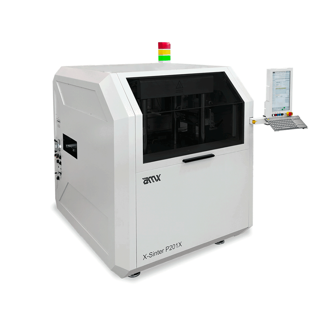
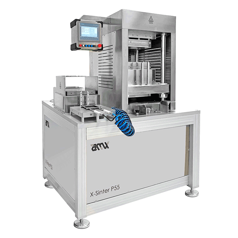


A new era process
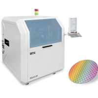
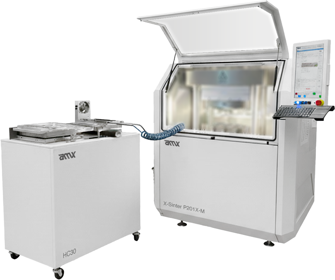
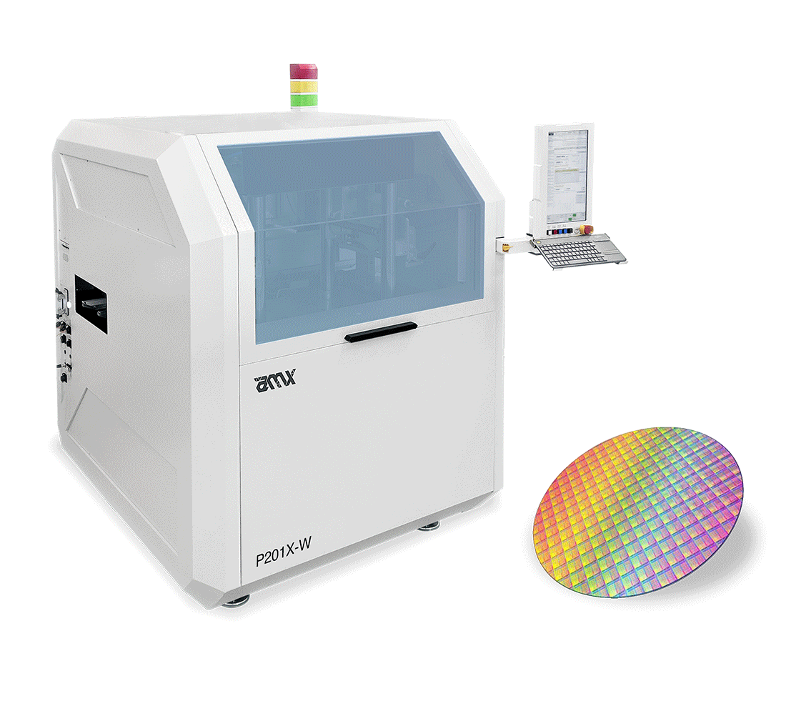
SiC on Wafer, Cu on SiC wafer, wafer lamination and wafer to wafer bonding by sintering. Processing entire wafers up to 12″ in diameter under controlled atmosphere.
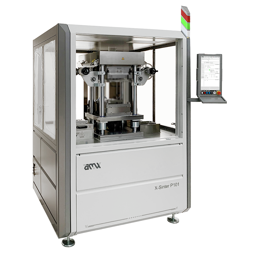
Heterogeneous Integration: Utilizes highly controlled systems, including the patented micropunch technology, to apply individually regulated pressure to multiple dies or components of varying height and force requirements across a single substrate area.
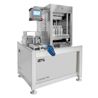
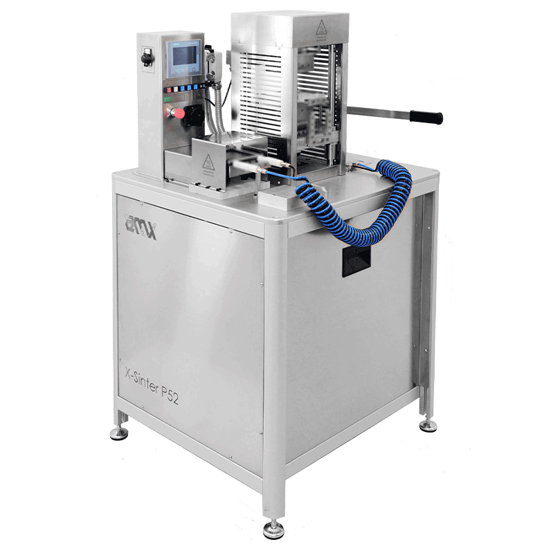
Following world’s trend, AMX developed a new range of product involving new range of processes to be evaluated in close collaboration with customers based on their final application needs.
IC to wafer bonding, wafer to wafer pressure sintering, SiC to wafer, polymeric film lamination on wafer are among the new challenges that AMX is currently focusing on.
Heterogeneous Integration: Utilizes highly controlled systems, including the patented micropunch technology, to apply individually regulated pressure to multiple dies or components of varying height and force requirements across a single substrate area.
Following world’s trend, AMX developed a new range of product involving new range of processes to be evaluated in close collaboration with customers based on their final application needs.
IC to wafer bonding, wafer to wafer pressure sintering, SiC to wafer, polymeric film lamination on wafer are among the new challenges that AMX is currently focusing on.